Arpelier
A visual workspace that turns semiconductor process flows into real-time 3D device structures
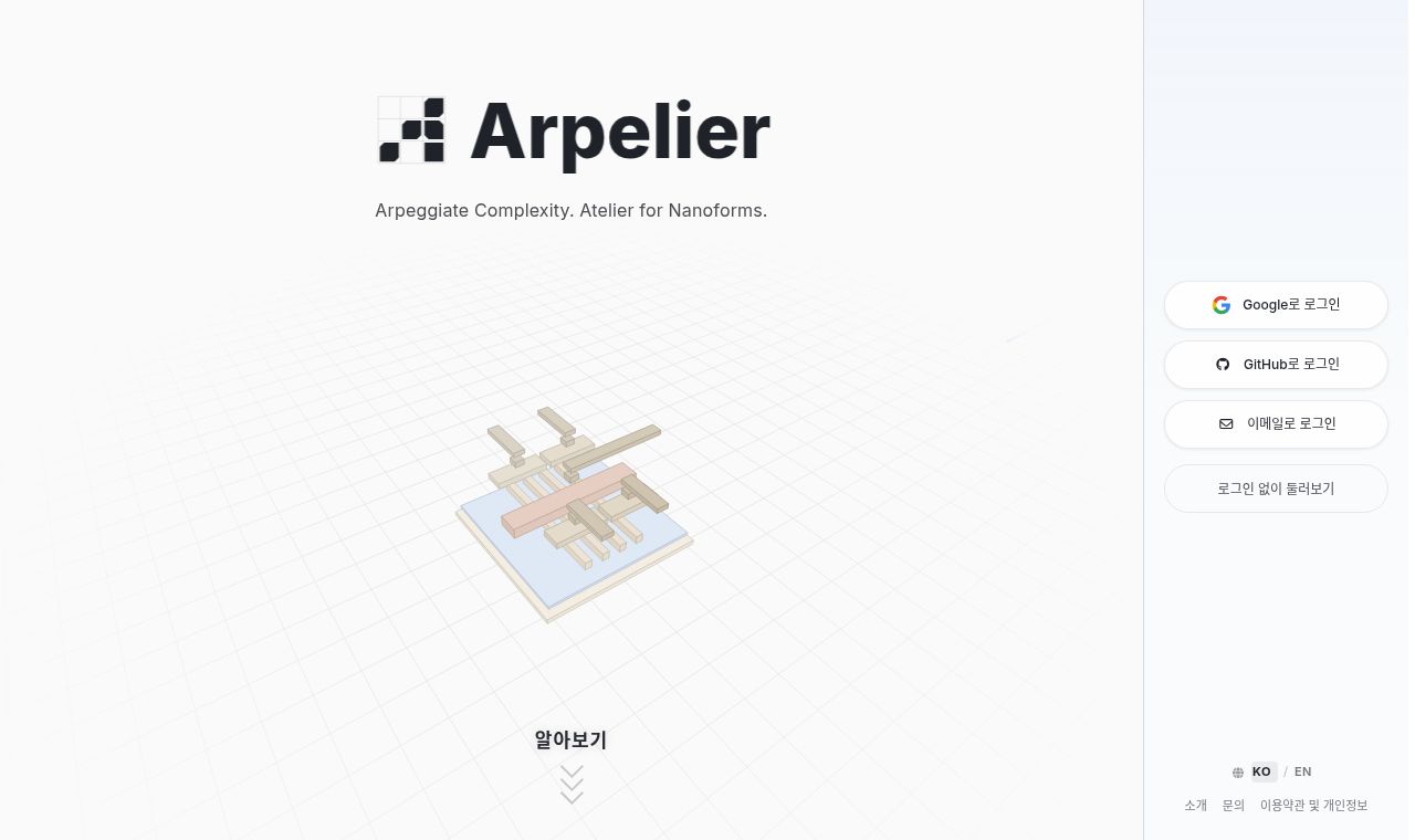 SITE CAPTURE
Based on information published on the service's website. Selection and review policy
WHAT IT DOES
What does it do?
Adding or editing a process step changes the 3D structure at that point and in subsequent steps in real time. Users can explore material composition, formation history, structural changes, and connections within the process context. They can learn from official examples and share or publish their own projects.
KEY FEATURES
Key features
- Generate 3D device structures from process flows
- Update subsequent structures in real time when a process step changes
- Explore structures through Composition, Provenance, Change, and Connect views
- Learn processes and the tool through official examples
- Share projects and set their visibility
- Prepare structure images for presentations
EDITOR'S NOTE
Why did it stand out?
It brings the manual work of separately drawing and explaining cause and effect between processes and structures into a single flow. Process edits propagate to later structures, making it especially useful for reviewing ideas and teaching.